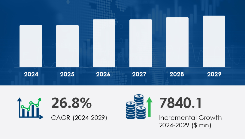
The Fan-Out Wafer Level Packaging (FOWLP) Market is projected to experience substantial growth between 2025 and 2029, driven by the demand for compact and high-performance electronic components. In 2024, the market was valued at USD 7.84 billion and is forecast to grow at a CAGR of 26.8%, continuing its upward trajectory through 2029. As the demand for miniaturized, high-performance electronics accelerates across industries, FOWLP is emerging as a pivotal technology in next-generation semiconductor packaging.
For more details about the industry, get the PDF sample report for free
One of the primary drivers of this market is the increasing demand for compactly designed electronics across industries such as consumer electronics, autonomous vehicles, data centers, and renewable energy. As device miniaturization becomes more critical, fan-out wafer level packaging (FOWLP) plays a vital role in addressing spatial constraints while enhancing functionality. Notably, miniaturized ICs using 14nm, 10nm, and 7nm nodes have become increasingly prevalent, enabling multiple functionalities within a single chip. This is essential for applications such as autonomous cars, AI chips, and in-vehicle infotainment systems, all of which rely on high-performance ICs in tight physical spaces. As such, FOWLP supports growing demand for energy efficiency and form factor reduction, making it a cornerstone in next-gen semiconductor packaging strategies.
A major trend influencing the Fan-Out Wafer Level Packaging Market is the increasing integration of semiconductor ICs in automobiles. The rise of electric and autonomous vehicles has accelerated the adoption of advanced packaging solutions like UHD fan-out and mega pillar plating. Automotive OEMs are integrating machine learning algorithms, RF modules, and AI chipsets into their vehicles, necessitating packaging that supports high-density interconnects and minimal thermal dissipation. The push toward smarter, more connected vehicles underscores the demand for footprint-sensitive, power-efficient solutions—a demand that FOWLP is uniquely positioned to meet.
The Fan-Out Wafer Level Packaging (FOWLP) Market is rapidly evolving as demand grows for compact electronics and high-performance computing solutions across industries. Fan-out packaging and wafer-level packaging offer critical benefits such as enhanced thermal performance, improved electrical characteristics, and support for miniaturized components. These technologies are particularly valuable in sectors deploying IoT devices, mobile devices, and autonomous vehicles, where size, speed, and power efficiency are crucial. Key architectural advancements like redistribution layers and through InFO Vias enable seamless chip integration and are instrumental in 3D packaging and 2D packaging structures. Applications in automotive ICs, including ADAS systems, benefit from robust design considerations and enhanced reliability. Simultaneously, high-bandwidth memory and system-in-package configurations are gaining traction in markets like edge computing, cloud systems, and artificial intelligence, as they address the growing need for faster data processing. Material and process innovations such as no-substrate solutions, FinFET technology, and HMI technology further drive improvements in packaging density and functionality.
The Fan-Out Wafer Level Packaging Market is segmented by:
Technology:
High density
Standard density
Type:
200 mm
300 mm
Panel
Application:
Consumer electronics
Automotive
Defense and aerospace
Medical
Others
Product Type:
Fan-out WLP
Through silicon via
Integrated passive device
Fan-in WLP
The high-density technology segment is forecast to be the market leader during the 2025–2029 period. This segment, valued at USD 1.76 billion in 2019, has demonstrated steady growth due to increasing use in application processor engines (APEs) and high-performance computing. FOWLP in this segment features over 200 external I/Os with sub-8µm line/space precision, making it ideal for neural network processors, GPUs, CPUs, and FPGAs. Analysts note that its advantages in supporting memory-on-logic architectures and machine learning workloads are fueling widespread adoption across industries demanding more bandwidth and computing power. This trend is further reinforced by rising investments in data centers and AI infrastructure, both of which require efficient, compact packaging.
Regions covered:
North America
Europe
APAC
South America
Middle East and Africa
APAC is expected to dominate the Fan-Out Wafer Level Packaging Market, accounting for 75% of global market growth during the forecast period. The region’s leadership is attributed to the presence of major OSAT companies and foundries, including nepes, ASE Technology Holding Co. Ltd., and Changdian Technology. ASE offers both Chip-First and Chip-Last fan-out packaging formats, optimized for components like FPGAs, RF modules, and GPUs, enabling thermal efficiency and reduced power loss. APAC’s manufacturing ecosystem supports the full range of FOWLP applications—from MEMS and power modules to microcontrollers—making it the region with the most dynamic and diverse growth in this segment.
See What’s Inside: Access a Free Sample of Our In-Depth Market Research Report.
Despite its growth potential, the Fan-Out Wafer Level Packaging Market faces a notable challenge: increased production costs due to warpage. Warpage occurs during the molding process, where differential shrinkage deforms the wafer surface, leading to wasted materials and reduced yield rates. This structural distortion is especially problematic in high-density applications, where precision is critical. As a result, manufacturing costs rise, and production complexity increases, potentially impeding widespread FOWLP adoption. Companies are attempting to address this issue by investing in protected fan-out technology and advanced process controls, yet the manufacturing complexity and thermal constraints remain significant hurdles to overcome.
Market research highlights the transition from traditional wafer sizes to 300mm wafers, with select niche applications still utilizing 200mm wafers. A key trend is the emergence of panel-level packaging and large panel processing techniques, which aim to reduce costs and enable high-volume manufacturing. Both standard-density packaging and high-density packaging are being adapted depending on device requirements, with panel packaging offering scalability for mass production. The demand for cost-effective packaging solutions has led to the rise of advanced packaging strategies that balance performance with manufacturability. However, technical challenges such as warpage control, die shift, and yield optimization remain crucial to commercial viability. In sectors like 5G applications, wireless communication, and evolving telecommunication standards, packaging design directly impacts signal performance and reliability. Moreover, the increasing use of multi-chip modules in various electronic systems underscores the need for robust, scalable solutions tailored for next-gen connectivity and computing platforms.
Analysis of the FOWLP market reveals a strong convergence of material science, semiconductor engineering, and system-level design to meet the demands of next-generation electronic applications. As the industry pushes toward lower power consumption, higher speeds, and form-factor reduction, fan-out and panel-level innovations are expected to play a central role. Continuous R&D investments, especially in AI, 5G, and edge computing, are poised to accelerate market adoption, shaping the future of packaging technologies in high-growth application areas.
Key players are actively pursuing innovative strategies and partnerships to secure competitive advantages in the Fan-Out Wafer Level Packaging Market. Analysts emphasize that companies leveraging heterogeneous integration and advanced design flexibility will be best positioned to capitalize on the growing demand for high-performance, compact, and thermally resilient ICs.
1. Executive Summary
2. Market Landscape
3. Market Sizing
4. Historic Market Size
5. Five Forces Analysis
6. Market Segmentation
6.1 Technology
6.1.1 High density
6.1.2 Standard density
6.2 Type
6.2.1 200 mm
6.2.2 300 mm
6.2.3 Panel
6.3 Application
6.3.1 Consumer electronics
6.3.2 Automotive
6.3.3 Defense and aerospace
6.3.4 Medical
6.3.5 Others
6.4 Product Type
6.4.1 Fan-out WLP
6.4.2 Through silicon via
6.4.3 Integrated passive device
6.4.4 Fan-in WLP
6.5 Geography
6.5.1 North America
6.5.2 APAC
6.5.3 Europe
6.5.4 South America
6.5.5 Middle East And Africa
7. Customer Landscape
8. Geographic Landscape
9. Drivers, Challenges, and Trends
10. Company Landscape
11. Company Analysis
12. Appendix
Safe and Secure SSL Encrypted
One user only.
Quick & easy download option
Unlimited user access (Within your organization).
Complimentary Customization Included
*For Enterprise license, go to checkout page
![]() Get the report (PDF) sent to your email within minutes.
Get the report (PDF) sent to your email within minutes.

