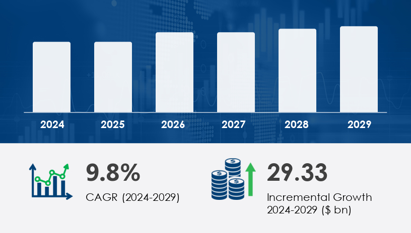
The semiconductor advanced packaging market is entering a transformative era, poised to expand by USD 29.33 billion from 2025 to 2029, at an impressive CAGR of 9.8%, according to industry forecasts. This surge is underpinned by escalating demand for compact, power-efficient integrated circuits (ICs) and the increasing adoption of these technologies in industries such as automotive, consumer electronics, and high-performance computing (HPC).As Moore’s Law begins to hit physical limitations, advanced packaging technologies are becoming the next frontier for innovation—offering the necessary improvements in performance, miniaturization, and power efficiency. These solutions are instrumental in enabling new functionalities like ADAS systems in electric vehicles, AI-enabled devices, and data center processors.For more details about the industry, get the PDF sample report for free
A comprehensive view of the market’s projected growth to 2029
Insights into key players and strategic initiatives
An overview of technological innovations in packaging
Regional market dynamics and opportunities
Emerging trends driving the future of semiconductors
Competition is intensifying among industry leaders striving to innovate and capture market share. Here are some prominent players:
Amkor Technology Inc. – Known for advanced BGA and thin-package solutions tailored for miniaturized electronics.
ASE Technology Holding Co. Ltd. – A global leader offering flip chip and wafer-level packaging (WLP).
Intel Corp. – Investing heavily in 3D packaging and high-performance computing applications.
TSMC (Taiwan Semiconductor Manufacturing Co. Ltd.) – Driving innovations in Fan-Out Packaging and 2.5D/3D integration.
Samsung Electronics Co. Ltd. – Focused on heterogeneous integration and silicon photonics.
Get more details by ordering the complete report
The semiconductor advanced packaging market is segmented by device type, technology, application, end-user, and region:
Analog and Mixed ICs – Valued at USD 9.92 billion in 2019; projected to see major gains.
MEMS and Sensors
Logic and Memory Devices
Wireless Connectivity Devices
CMOS Image Sensors
Flip Chip
Fan-In WLP
2.5D/3D Packaging
Fan-Out WLP
High-Performance Computing
Internet of Things (IoT) Devices
Consumer Electronics
Telecommunications
Automotive
Telecom
Consumer Electronics
Advanced packaging solutions such as TSV (Through-Silicon Via) and interposer technologies are particularly valuable in logic devices and HPC, where bandwidth, signal integrity, and thermal management are critical.
Electric and autonomous vehicles are driving the need for compact, multifunctional semiconductor ICs. Features like collision detection, GPS navigation, and infotainment systems rely heavily on advanced packaging for performance and miniaturization.
As chipmakers battle physical scaling limits, technologies like 3D ICs, silicon photonics, and heterogeneous integration are vital to meet the rising need for performance within smaller footprints.
Advancements in inorganic substrates (glass, silicon), EUV lithography, and failure analysis tools enhance packaging yield and enable precision reliability testing. Design for manufacturing (DFM) and automation streamline processes, reducing time to market.
While innovation is abundant, so are the challenges. Warpage during wafer processing can result in high rejection rates and added cost. Additionally, the need for specialized equipment and materials raises barriers for new entrants.
These companies are utilizing strategic alliances, geographic expansion, and M&A to maintain competitive advantages. Partnerships that foster shared R&D and IP protection are essential in this rapidly evolving landscape.
For more details about the industry, get the PDF sample report for free
The Asia-Pacific region, particularly Taiwan, South Korea, Japan, and China, is projected to contribute 34% of the global growth through 2029. Major investments from TSMC, Samsung, SMIC, and leading OSAT (Outsourced Semiconductor Assembly and Test) companies are fueling this growth.
Taiwan: Home to TSMC, a hub for consumer electronics and advanced chip packaging.
South Korea: Dominated by Samsung and SK HYNIX, focusing on memory bandwidth and 3D packaging.
Japan: A stronghold in material science and semiconductor manufacturing equipment.
North America leads in high-performance computing applications, thanks to players like Intel and AMD.
Europe is advancing in automotive semiconductors, particularly in Germany and France, emphasizing vehicle automation and electrification.
Middle East and Africa
South America
Rest of World (ROW)
The Semiconductor Advanced Packaging Market is rapidly evolving, driven by the demand for high-performance, compact, and energy-efficient electronic systems. Technologies like flip chip, fan-out WLP, 2.5D packaging, and 3D ICs are becoming central to next-generation chip designs. Applications such as CMOS image sensors, MEMS sensors, logic devices, and memory devices are adopting these advanced packaging methods to enhance processing capabilities and reduce form factors. The rise in wireless connectivity needs is fueling innovations in system-in-package and chiplet integration solutions, with cutting-edge hybrid bonding techniques supporting more robust interconnectivity. Key processes like wafer bumping, die attach, and ball grid array mounting play crucial roles in manufacturing efficiency. Packaging solutions such as embedded die, high-density interconnects, and advanced substrates including organic substrates and leadframe packaging are essential for meeting modern design requirements. Additionally, materials such as encapsulation resins, bonding wire, and ceramic packages are vital for improving thermal management and durability across various end-user applications.
Get more details by ordering the complete report
Key Statistics (2025–2029 Forecast):
Market Growth: +$29.33 Billion
CAGR: 9.8%
Top Growth Segments: Analog ICs, 3D Packaging, Automotive Electronics
Leading Region: Asia-Pacific (34% share)
Silicon Photonics – Transforming data transfer rates for HPC and cloud computing.
Heterogeneous Integration – Allows multiple chips with different functions in one package.
Machine Learning & AI Integration – Optimizing design and production pipelines.
Design Automation & Assembly Line Optimization – Critical for reducing time-to-market and manufacturing defects.
For more details about the industry, get the PDF sample report for free
Research reveals that advanced packaging technologies are critical for supporting high-performance applications in power devices, RFID chips, AI processors, and HPC chips, especially within the context of expanding 5G modules and IoT devices. The automotive sector is also benefiting from robust solutions for automotive ICs, reflecting the growing importance of miniaturized electronics in electric and autonomous vehicles. Innovations in heterogeneous integration, wafer-level packaging, and the development of thin wafers are enabling the rise of multi-chip modules with improved signal integrity and power efficiency. Additionally, the market is seeing an increased demand for compact ICs, high-frequency chips, and nano-sized chips, all of which are fundamental to space-constrained and high-speed applications. The synergy between chip packaging advancements and the broader innovation in integrated circuits and semiconductor dies highlights the strategic importance of packaging as not just a manufacturing step, but a performance enabler in modern semiconductor design.
As the demand for smarter, faster, and more compact devices grows, the semiconductor advanced packaging market is set to become a cornerstone of technological evolution. From autonomous vehicles to AI-driven cloud computing, advanced packaging will be the enabling force behind next-generation electronics.Companies that can balance innovation with cost-efficiency, navigate production challenges, and leverage strategic alliances will lead this revolution. The market is dynamic, innovation-rich, and ripe with opportunities for those ready to invest in the future of chipmaking.
Get more details by ordering the complete report
Safe and Secure SSL Encrypted
One user only.
Quick & easy download option
Unlimited user access (Within your organization).
Complimentary Customization Included
*For Enterprise license, go to checkout page
![]() Get the report (PDF) sent to your email within minutes.
Get the report (PDF) sent to your email within minutes.

