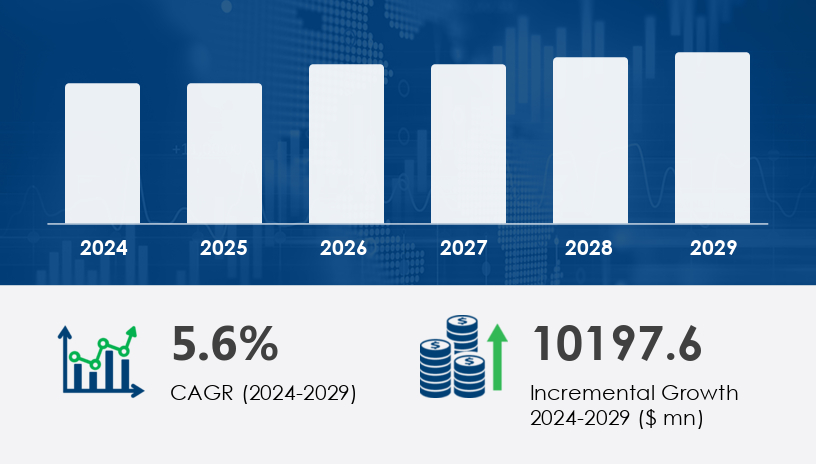
The semiconductor packaging materials market is forecast to grow significantly, reaching a total value increase of USD 10.2 billion between 2024 and 2029, with a compound annual growth rate (CAGR) of 5.6%. This growth is fueled by the rapid miniaturization of electronics and the rising demand for efficient, high-performance semiconductor packages across various sectors. In 2024, the market stood robustly on the backbone of increasing applications in consumer electronics, automotive systems, and data center infrastructure. As innovation accelerates in the Internet of Things (IoT) and system integration, semiconductor packaging materials are playing a critical role in performance, durability, and energy efficiency.
For more details about the industry, get the PDF sample report for free
A primary driver of the semiconductor packaging materials market is the miniaturization of electronic devices combined with the proliferation of IoT applications. As devices become more compact yet powerful, the need for advanced semiconductor packaging materials has surged. Technologies such as System-in-Package (SiP), 3D packaging, and Chip-on-Board (CoB) are becoming increasingly essential. For instance, flip-chip packaging, which uses conductive bumps to connect chips with substrates, supports high system density and performance. These innovations enable integration of multiple components in a single unit, improving performance while reducing size and power consumption. According to the report, these advanced packaging solutions are not only critical to product performance but also to reducing costs and boosting yield in manufacturing.
One of the most notable trends in the semiconductor packaging materials market is the growing adoption of lead-free, environmentally compliant packaging solutions. Companies are transitioning to materials like matte tin and nickel-palladium-silver alloys to comply with RoHS standards. Additionally, the shift toward flip-chip and SiP packaging technologies is accelerating due to their superior thermal management and system integration capabilities. These technologies are crucial for supporting high-performance computing in data centers and mobile devices. The market is also seeing an increase in demand for thermal interface materials, gap pads, and underfill compounds that manage heat and enhance durability. As heterogeneous integration gains traction, semiconductor manufacturers are leveraging these innovations to stay competitive in a fast-evolving industry.
The Semiconductor Packaging Materials Market is a vital component of the broader semiconductor ecosystem, enabling the protection, connectivity, and performance enhancement of integrated circuits and embedded processors across a wide range of applications. Core processes like semiconductor packaging, chip packaging, and wafer-level packaging rely on diverse packaging materials such as lead-free solders, underfill materials, and encapsulation resins to ensure mechanical integrity and environmental resistance. Packaging solutions like flip chip, 3D packaging, fan-out WLP, and system-in-package are central to achieving miniaturization and space optimization, especially in compact designs. Materials like organic substrates provide the necessary mechanical support while maintaining robust electrical performance. Technologies like chip-on-board, ball grid array, and leadframe packaging support a variety of high-density integration formats for MEMS devices, RFID packaging, and power devices, each requiring unique structural and thermal characteristics.
Material
Organic substrates
Lead frames
Bonding wires
Ceramic packages
Others
End-user
Consumer electronics
Automotive
Medical devices
Communication and telecom
Others
Technology
Grid array
System-in-package (SiP)
Others
The organic substrates segment leads the semiconductor packaging materials market in terms of growth. Valued at USD 11.48 billion in 2019, this segment has shown steady growth and is projected to continue on this trajectory through 2029. Organic substrates are widely used due to their affordability, mechanical strength, and compatibility with high-density circuit design. These substrates support advanced packaging techniques like SiP and flip-chip, which require reliable thermal and mechanical performance. Analysts note that the proliferation of compact, high-performance devices in mobile and consumer electronics is a key reason behind the rising demand for organic substrates. Their ability to meet the structural and electrical requirements of miniaturized devices positions them as the backbone of modern semiconductor packaging.
Regions Covered
North America
Europe
APAC
South America
Rest of World (ROW)
APAC dominates the semiconductor packaging materials market, contributing approximately 73% to global market growth during the 2025–2029 forecast period. This region benefits from strong manufacturing capabilities, particularly in countries like China, Japan, South Korea, and Taiwan. The high demand for smartphones, consumer electronics, and computing devices continues to drive packaging innovation in the region. According to analysts, China's favorable economic policies and large-scale production infrastructure have attracted global semiconductor companies to establish operations in the country. Moreover, South Korea’s government announced a USD 12.5 billion investment in March 2025 to bolster advanced packaging technologies. This reinforces APAC’s leadership position, both in terms of production and technological innovation.
See What’s Inside: Access a Free Sample of Our In-Depth Market Research Report
A key challenge confronting the semiconductor packaging materials market is its capital-intensive nature. The cost of manufacturing equipment—such as photolithography tools, etching systems, and wafer thinning machinery—often reaches millions of dollars. These high upfront investments create entry barriers for smaller players and increase financial risk amid market volatility. Furthermore, the need for advanced packaging techniques like wafer-level packaging (WLP), thin film deposition, and heterogeneous integration adds complexity and cost to production. While epoxy resins and mold compounds help improve efficiency and thermal stability, their implementation still requires substantial operational investment. Supply chain disruptions and fluctuations in raw material pricing further compound these challenges, putting pressure on manufacturers to optimize both cost and quality.
Market research shows that packaging advancements are directly tied to the needs of high-functioning electronics and emerging device applications. Trends such as 3D integration, heterogeneous integration, and advanced packaging are critical in driving performance improvements in AI chips, IoT devices, and automotive ICs. The emphasis on signal integrity, low power, and high performance has led to the adoption of bonding wire, copper wire, die attach, and wafer bumping technologies that ensure stable interconnects and reliability in harsh environments. In addition, thermal management and heat dissipation have become top priorities for manufacturers as 5G applications, consumer electronics, and smart devices push components to higher frequencies and tighter enclosures. Devices like wearable devices and compact sensors increasingly rely on efficient packaging solutions to support high-speed applications and reduce form factor constraints.
Research analysis reveals a strong industry pivot toward optimized materials and integration strategies that deliver on performance, efficiency, and cost targets. Innovations in electrical performance, space-conscious layouts, and energy-efficient designs are enabling faster time-to-market across sectors. As demand for smart, connected products grows, semiconductor packaging materials will remain at the forefront of enabling transformative technology in mobile, automotive, AI, and next-generation communications infrastructure.
The competitive landscape of the semiconductor packaging materials market is marked by technological innovation, strategic partnerships, and geographic expansion. Companies are focusing on high-performance materials and processes that improve integration, thermal management, and environmental compliance.
Recent innovations include:
Infineon Technologies AG launched a new Copper Flip Chip Technology in February 2024. This technology enhances power efficiency and processing performance, marking a leap forward in chip-level interconnect solutions.
Merck KGaA completed its USD 3.4 billion acquisition of Versum Materials in October 2024, strengthening its portfolio and market position in the semiconductor materials sector.
In March 2025, South Korea committed USD 12.5 billion toward semiconductor industry development, with a significant portion earmarked for packaging material innovations.
Companies like Amkor Technology Inc., ASE Technology Holding Co. Ltd., and DuPont de Nemours Inc. are investing in R&D and forming alliances to enhance capabilities in SiP, lead-free packaging, and 3D integration. The use of copper leadframe substrates, as seen in Amkor's offerings, reflects industry-wide efforts to meet performance, cost, and sustainability goals simultaneously.
1. Executive Summary
2. Market Landscape
3. Market Sizing
4. Historic Market Size
5. Five Forces Analysis
6. Market Segmentation
6.1 Material
6.1.1 Organic substrates
6.1.2 Lead frames
6.1.3 Bonding wires
6.1.4 Ceramic packages
6.1.5 Others
6.2 End-user
6.2.1 Consumer electronics
6.2.2 Automotive
6.2.3 Medical devices
6.2.4 Communication and telecom
6.2.5 Others
6.3 Technology
6.3.1 Grid array
6.3.2 System-in-package (SIP)
6.3.3 Others
6.4 Geography
6.4.1 North America
6.4.2 APAC
6.4.3 Europe
6.4.4 South America
6.4.5 ROW
7. Customer Landscape
8. Geographic Landscape
9. Drivers, Challenges, and Trends
10. Company Landscape
11. Company Analysis
12. Appendix
Safe and Secure SSL Encrypted
One user only.
Quick & easy download option
Unlimited user access (Within your organization).
Complimentary Customization Included
*For Enterprise license, go to checkout page
![]() Get the report (PDF) sent to your email within minutes.
Get the report (PDF) sent to your email within minutes.

