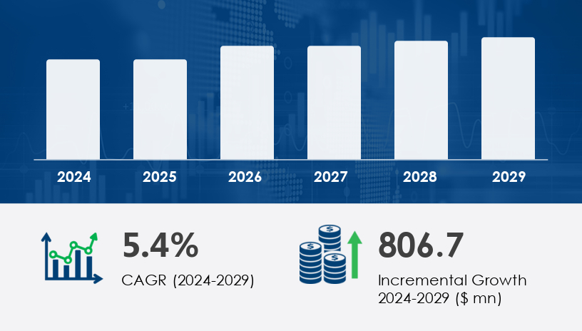
The Ion Implanter Market is a critical segment of the global semiconductor industry, enabling the production of advanced integrated circuits and electronic devices through precise doping of silicon wafers. Valued significantly in 2024, the market is projected to grow by USD 806.7 million during the forecast period, reaching a compound annual growth rate (CAGR) of 5.4% between 2024 and 2029.
For more details about the industry, get the PDF sample report for free
A major driver accelerating the growth of the Ion Implanter Market is the surge in demand for integrated circuits (ICs), which are essential to technologies such as artificial intelligence (AI), Internet of Things (IoT), autonomous vehicles, and Industry 4.0. Semiconductor manufacturers are investing heavily in new fabrication facilities to keep up with rising chip demand. For instance, Samsung recently began construction on a 5-nanometer fabrication plant in South Korea, aimed at expanding its foundry operations. This expanding infrastructure reflects how the need for high-performance ICs is pushing companies to scale up semiconductor production, directly boosting demand for ion implantation systems that are crucial for modifying the electrical properties of silicon wafers in the chip fabrication process.
An emerging trend shaping the Ion Implanter Market is the increasing adoption of carbon nanotubes across industrial applications. Known for their exceptional strength and superior electrical and thermal conductivity, carbon nanotubes are manufactured using ion implantation technologies, which deposit metal catalyst layers like nickel or cobalt to facilitate nanotube growth. This process, enabled by ion implanters, is vital in producing materials that are several times stronger than steel. As industries explore new applications for carbon nanotubes in electronics, aerospace, and advanced composites, the use of ion implantation to support their production is expected to further fuel market demand.
The Ion Implanter Market is critical to the advancement of semiconductor fabrication, enabling precise ion implantation processes that alter the electrical properties of silicon wafers to enhance device performance. Core to this are specialized systems like the high-current implanter, medium-current implanter, and high-energy implanter, each suited for different levels of substrate doping and semiconductor doping. Through methods such as plasma doping and beamline implanter technology, manufacturers can implement angular control, angle control, and dosimetry control for optimal accuracy. Applications include the doping of source/drain regions, halo implants, and the formation of isolation structures, all of which improve chip performance and conductivity modification. These techniques are essential in producing integrated circuits, microprocessor chips, and memory chips used across a variety of products. By mitigating issues like channeling effect and metal contamination, ion implanters ensure process consistency and effective wafer processing, especially in high-demand sectors like consumer electronics and telecommunications equipment.
By Technology:
High-current implanter
Medium-current implanter
High-energy implanter
By Application:
Semiconductors
Metal finishing
Others
By Type:
10–28nm
Sub-10nm
Above 28nm
The high-current implanter segment is expected to lead the market during the forecast period due to its superior precision and control in semiconductor manufacturing processes. Valued at USD 1.08 billion in 2019, this segment continues to gain momentum due to its suitability for halo implantation, which requires precise angular control and improved dosimetry. Analysts note that the low throughput of medium-current implanters at lower energies is driving the industry's shift toward high-current solutions. These systems are now preferred in producing complex semiconductor components found in consumer electronics, including smartphones, laptops, and 5G devices, where speed and accuracy are paramount.
Covered Regions:
North America
Europe
Asia-Pacific (APAC)
Rest of World (ROW)
The Asia-Pacific (APAC) region is projected to contribute 83% of the global Ion Implanter Market growth from 2025 to 2029. This dominance is attributed to the presence of major chip manufacturing hubs in countries like China, Japan, South Korea, Taiwan, and India. Notably, countries in the region are expanding their fabrication capabilities to meet the increasing demand for semiconductors across industries such as automotive, telecommunications, and consumer electronics. Analysts highlight that this regional expansion is being driven by the proliferation of 5G phones, smart devices, and data centers, all of which rely on semiconductors fabricated using ion implantation. The strong growth trajectory in APAC offers substantial opportunities for market players.
Despite robust growth, the Ion Implanter Market faces a significant challenge: the rising adoption of refurbished ion implanters. High initial investment costs for new systems—alongside the economic constraints of smaller manufacturers—have driven demand for previously owned, cost-effective equipment. These refurbished systems can often meet current performance standards after appropriate upgrades, particularly in emerging markets where budgets are limited. However, this trend threatens to suppress sales of new ion implanters, impacting revenue growth for original equipment manufacturers and shifting competitive dynamics within the industry.
Market research highlights the growing deployment of ion implanters in emerging electronics such as 5G phones, gaming consoles, and wireless access devices, where advanced doping enhances performance and energy efficiency. The technology is also expanding into specialized areas like automotive ICs, LED manufacturing, and photodiode fabrication, including applications in deep photodiode, pinned photodiode, and image sensors. The precision enabled by ion implanters supports innovations in transistor tuning, resist patterns, and angle control, all vital for maintaining nanometer-scale design rules. Outside semiconductors, ion implantation is seeing use in metal finishing and research into carbon nanotubes for future nanoelectronic applications. Additionally, its role in ensuring high throughput for fabrication facilities has made it a backbone for scaling global production. As demand surges, ion implantation continues to shape the competitive landscape of next-gen electronics manufacturing.
Analysis of the ion implanter market reveals strong momentum driven by miniaturization, 5G rollout, and next-gen sensor technologies. With advancements in beam control, angular precision, and contamination reduction, ion implanters are expected to remain vital tools for semiconductor innovation. Investments in fabrication efficiency, material science, and doping uniformity will shape the roadmap for the industry as it meets the demands of increasingly complex device architectures.
To remain competitive, leading companies in the Ion Implanter Market are focusing on product innovation and strategic partnerships. For instance, in March 2025, Axcelis Technologies, Inc. announced its Diamond Sponsorship of the Compound Semiconductor Asia Conference (CS Asia) 2025, with its CEO delivering the keynote address—a move that highlights its commitment to industry leadership. Earlier, in December 2024, Axcelis showcased its Purion™ and GSD Ovation™ Series at SEMICON Japan 2024, targeting emerging demand in Japan's semiconductor industry.
These developments reflect a larger trend of companies leveraging industry events, product showcases, and global exposure to maintain brand presence and attract clients. Analysts note that firms must prioritize energy efficiency, high-throughput capability, and user-friendly system design to capture market share, particularly amid rising competition from refurbished equipment and evolving semiconductor technologies.
1. Executive Summary
2. Market Landscape
3. Market Sizing
4. Historic Market Size
5. Five Forces Analysis
6. Market Segmentation
6.1 Technology
6.1.1 High-current implanter
6.1.2 Medium-current implanter
6.1.3 High-energy implanter
6.2 Application
6.2.1 Semiconductors
6.2.2 Metal finishing
6.2.3 Others
6.3 Type
6.3.1 10-28nm
6.3.2 Sub-10nm
6.3.3 Above 28nm
6.4 Geography
6.4.1 North America
6.4.2 APAC
6.4.3 Europe
6.4.4 ROW
7. Customer Landscape
8. Geographic Landscape
9. Drivers, Challenges, and Trends
10. Company Landscape
11. Company Analysis
12. Appendix
Safe and Secure SSL Encrypted
One user only.
Quick & easy download option
Unlimited user access (Within your organization).
Complimentary Customization Included
*For Enterprise license, go to checkout page
![]() Get the report (PDF) sent to your email within minutes.
Get the report (PDF) sent to your email within minutes.

